1 What is FPGA?
Field Programmable Gate Arrays formally known as FPGA.It is an alternative for implementation of digital logic in systems. They are prefabricated silicon chips that can be programmed electrically to implement any digital design. The first static memory-based FPGA (commonly called as SRAM based FPGA) was proposed by Wahlstrom in 1967. This architecture allowed for both logic and interconnection configuration using a stream of configuration bits. Later on the first commercial modern-era FPGA was introduced by Xilinx in 1984. It contained the low classic array of Configurable Logic Blocks (CLBs) and inputs/outputs. From that of first FPGA which contain 64 CLBs and 58 inputs and outputs , FPGAs have grown enormously in complexity. Today’s modern FPGA now can contain approximately 330,000 logic blocks and around 1100 inputs and outputs.
2 What are sub-parts/internal blocks of FPGA?
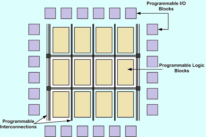
he basic architecture of FPGA consists of three major components: programmable logic blocks which implements the logic functions, programmable routing (interconnects) to implement these functions and I/O blocks to make off-chip connections. An illustration of typical FPGA architecture is shown in figure
Fig.1 Internal Architecture of FPGA
A. Programmable Logic blocks-
The purpose of programmable logic block in a FPGA is to provide the basic computation and storage elements used in digital systems. The basic logic element contains some form of programmable combinational logic, a flip-flop or latch and some fast carry logic to reduce area and delay cost to it could be entire processor. In addition to a basic logic block, many modern FPGAs contains a heterogeneous mixture of different blocks, some of which can only be used for specific functions, such as dedicated memory blocks, multipliers or multiplexers; of course, configuration memory is used throughout the logic block to control the specific function of each element within the block
B. Programmable Interconnect-
The programmable routing in an FPGA provides connections among logic blocks and I/O blocks to complete a user defined design. It consists of multiplexers, pass transistors and tri-state buffers, which forms the desired connection. Generally, pass transistors and multiplexers are used within a logic cluster to connect the logic elements together while all three are used for more global routing structures. Several global routing structures have been used in FPGAs as: island-style, cellular, bus-based and registered (pipelined) architectures.
C. Programmable I/O-
The media or mean required to interface the logic blocks and routing architectures to the wide range of external components to FPGA called as I/O pads or programmable I/O. The I/O pad and surrounding supporting logic circuitry forms as an I/O cells. These cells are important components of an FPGA and consume a significant portion (approximately 40%) of FPGAs area. The design of I/O programmable blocks is challenging as there is a great diversity in the supply voltage and reference voltage standards. One of the most important decisions in I/O architecture design is the selection of standards that will be supported. This involves carefully made trade-offs because, unlike LUTs, which can implement any digital functions, I/O cells can generally implement the voltage standards selected by designers. Supporting large number of standards can increase the silicon area required for I/O cells significantly. Additionally to support more number of standards pin capacitance may increase with more number of pins, which can limit the performance.
Over the time, the basic FPGA architecture has been further developed through the addition of more specialised programmable functional blocks. The special function blocks like- embedded memory (Block RAMs), arithmetic logic (ALUs), multipliers, DSP-48 and even embedded microprocessors have been added due to a frequent need of such resources for an application. The result is that many FPGAs have the heterogeneous mixture of resources than early FPGAs.
As FPGA is Reconfigurable Architecture,while programming FPGA we can have three type of programming approach depending on the time and resource requirement of programmer/user.The architectures are discussed as below
A.Serial Approach:
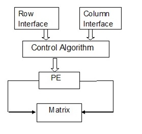
When application demands for minimum resource utilization but can permit longer execution time then this type of approach is preferred.This approach is also called as ‘Single PE approach’.
Fig 2:Serial approach
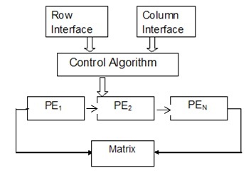
B.Parallel Approach:When application demands for faster execuation of code irrespective of hardware resource utilization, then this type of approach is preferred.This approach is also called as ‘Systolic approach’ or ‘nPE approach’.
Fig 3:Parallel Approach
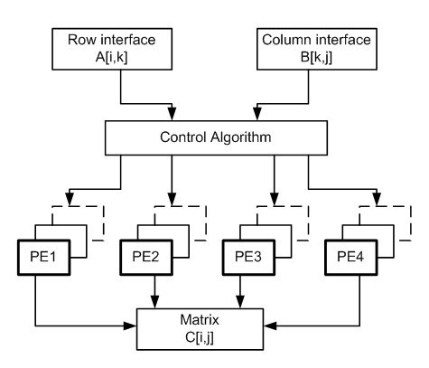
C:Iterative Approach: For optimization of both resource utilization and execuation time and to improve area/speed metric this approach is preferred.


good information iam a learner of fpga
LikeLike
Thanks!!
LikeLike
thank you your kind service
LikeLike
Very nice information for beginners. Keep it up thank you.
LikeLike
truly helpful…..
LikeLike
Thanks for the information…You are doing a good job..keep it up!
LikeLike
thanks…….
LikeLike
Thanks… it is more helpful
LikeLike
VERY GOOD INFORMATION about FPGAs
LikeLike
Thanks….!
LikeLike
pls post verilog tutorial pls pls vedika
LikeLike
Good and easy to understand material . . Keep it up 🙂
hope to see more 🙂
LikeLike
it was nice and excellent……………please update with the trendy manner
LikeLike
thanks a lot…………:)…….keep up this work
LikeLike
Informative content
LikeLike
Good piece of information.
LikeLike
nice and neatly understood…
keep up the good work
LikeLike